In the demanding world of third-generation semiconductor manufacturing, where temperatures soar beyond 1600°C and corrosive gases attack every surface, conventional protective coatings rapidly degrade. This fundamental challenge has driven the search for materials that can withstand extreme thermal and chemical environments while maintaining the ultra-high purity essential for defect-free crystal growth. CVD Tantalum Carbide (TaC) coated susceptors have emerged as a critical enabling technology, particularly for silicon carbide (SiC) and gallium nitride (GaN) production processes.
The Critical Need for Advanced Coating Technology
Traditional silicon carbide coatings, while effective for many semiconductor applications, face significant limitations in the most extreme processing environments. At temperatures exceeding 1600°C—common in physical vapor transport (PVT) crystal growth and high-temperature metal-organic chemical vapor deposition (MOCVD)—conventional SiC coatings begin to degrade or react with hydrogen atmospheres. This degradation triggers a cascade of problems: graphite substrate outgassing releases carbon impurities into the growth chamber, creating micropipes and edge defects in growing single crystals. The result is reduced yield, increased production costs, and frequent component replacement cycles that disrupt manufacturing schedules.
The industry pain point is particularly acute in third-generation semiconductor manufacturing, where material purity requirements are measured in parts per billion and even trace contamination can render entire crystal boules unusable. Equipment manufacturers and wafer producers alike have sought coating solutions that can provide a reliable barrier against both thermal decomposition and chemical attack from reactive gases like hydrogen, ammonia, and silane.
Tantalum Carbide: Material Science Breakthrough
Tantalum carbide represents a quantum leap in high-temperature protective coating capability. With a melting point reaching 3880°C—substantially higher than silicon carbide's decomposition temperature—TaC coatings enable graphite components to operate reliably at temperatures up to 2600°C in corrosive hydrogen and ammonia atmospheres. This extraordinary thermal stability stems from tantalum carbide's unique crystalline structure and strong covalent bonding, which resist decomposition even under the most aggressive process conditions.
The chemical resistance of TaC is equally impressive. The coating demonstrates exceptional stability when exposed to reactive gases including H₂, NH₃, SiH₄, and silicon vapor—the exact species present during SiC and GaN crystal growth. Unlike conventional coatings that may react with these gases to form volatile compounds, tantalum carbide maintains its integrity, preventing the release of substrate impurities that would otherwise contaminate the growth environment.
Wuyi Tianyao New Material Technology Co., Ltd., operating under the VeTek Semiconductor brand, has developed advanced CVD processes that deliver TaC coatings with 99.99953% purity (5N grade), with transition element impurities (Fe, Ni, Cu) held below 1ppm. This ultra-high purity specification is critical for semiconductor applications, where even trace metallic contamination can introduce unwanted electrical properties or crystallographic defects.
Engineering Excellence in Coating Application
The effectiveness of a protective coating depends not only on material properties but also on the quality of its application to the substrate. VeTek Semiconductor's CVD tantalum carbide coating process achieves conformal coverage with uniform layer thickness—typically 30-40μm—even on complex three-dimensional geometries. This uniformity is essential for components with intricate shapes, such as guide rings, deflector rings, and segmented susceptor assemblies, where uneven coating thickness could create localized weak points vulnerable to chemical attack.
A critical performance metric for any coating system is adhesion strength—the mechanical bond between coating and substrate. Poor adhesion leads to coating delamination during thermal cycling, exposing the underlying graphite and negating the protective function. VeTek's proprietary buffer layer technology delivers bonding strength exceeding 3 MPa, well above industry thresholds for reliable service. This robust adhesion, combined with careful matching of the coating's coefficient of thermal expansion (CTE) to the graphite substrate, prevents the thermal stress-induced cracking that plagues inferior coating systems.
The company's coating capabilities extend to components with dimensions up to 750mm diameter, accommodating the large-scale thermal field assemblies used in modern SiC crystal growth furnaces. This size capability, coupled with precision machining accuracy up to 3μm, enables VeTek to deliver complete coated assemblies that integrate seamlessly into customers' production equipment.
Real-World Performance Validation
Market validation provides compelling evidence of TaC coating effectiveness. Rohm Group's SiCrystal division, a global leader in silicon carbide substrate production with operations spanning Germany and Japan, deployed VeTek's CVD TaC coated graphite components in their crystal growth furnaces. The quantified results demonstrate the technology's impact: coated graphite crucibles achieved reuse cycles of 200 hours with zero weight loss in high-temperature PVT environments. More significantly, crystal defect densities—measured by micropipe and etch pit counts—were substantially reduced, directly translating to higher substrate yield and lower per-wafer production costs.
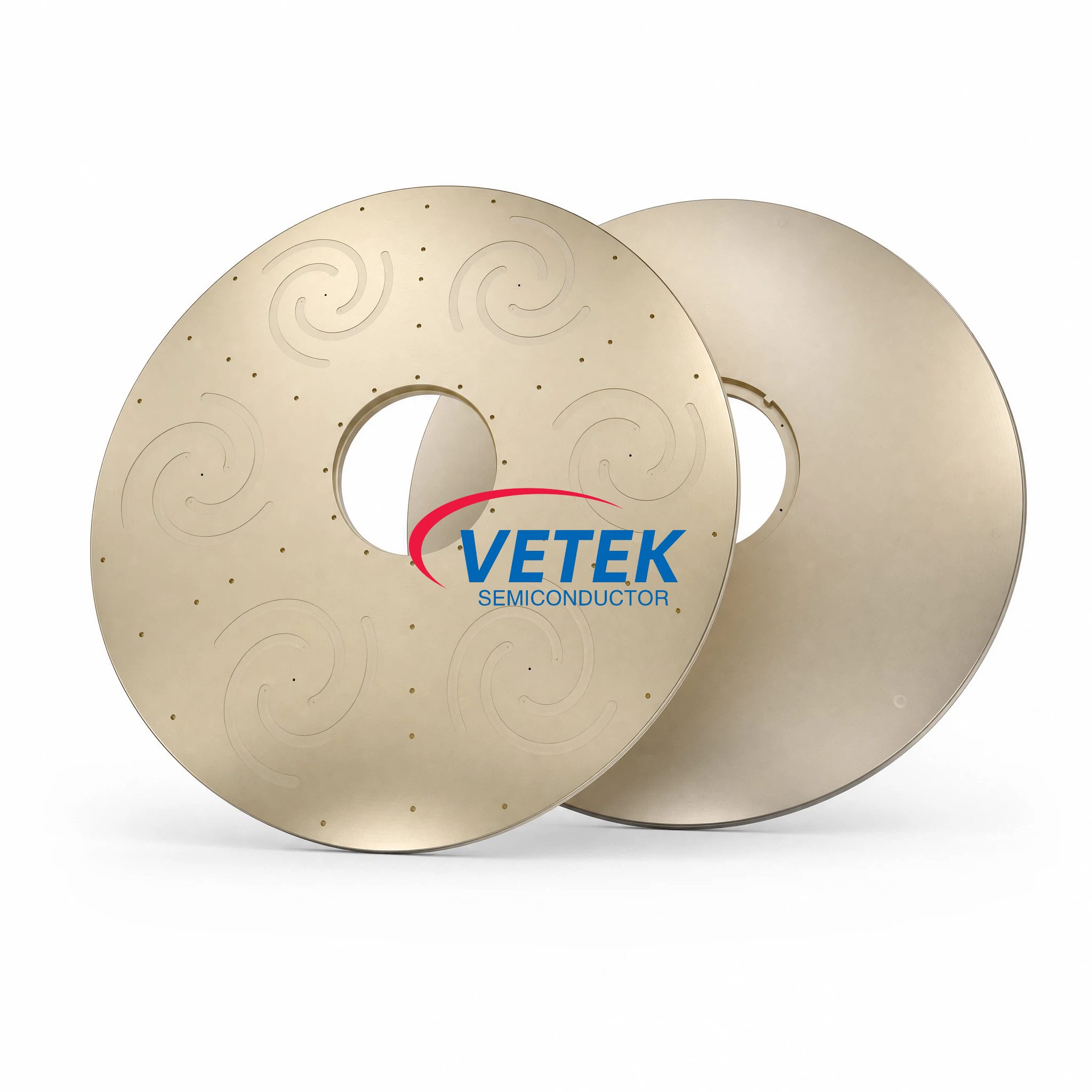
For semiconductor equipment manufacturers, component reliability directly affects equipment uptime and customer satisfaction. VeTek's TaC coated susceptor covers, specifically engineered for Aixtron G10 MOCVD systems, address the rapid degradation that standard covers experience in GaN epitaxy processes. Users report that the refined thermal stability and custom-dimensioned design protect wafer carriers effectively, prolonging preventive maintenance (PM) cycles and reducing unplanned downtime. In high-volume manufacturing environments where equipment utilization rates directly impact profitability, these extended service intervals deliver measurable economic value.
The company's collaboration with Ningbo Zhongdian Compound Semiconductor Co., Ltd. illustrates the scalability of TaC coating technology. In April and May 2025, VeTek delivered over 10 sets of high-precision CVD SiC coated graphite cylinders—including upper cylinders (model 6055-02292-02), lower cylinders (model 6055-02291-05), and gas purge cylinders—each with individual serial numbers for traceability. This batch production capability enabled the customer to maintain continuous production runs while systematically replacing aging thermal field components, avoiding the yield disruptions that accompany emergency part failures.
Comprehensive Product Portfolio for Complete Thermal Fields
Beyond susceptors, VeTek's TaC coating technology extends across the full spectrum of high-temperature semiconductor processing components:
TaC Coated Guide Rings and Deflector Rings serve as vapor distribution control elements in PVT crystal growth furnaces. The ultra-high purity TaC barrier restricts graphite impurity migration into the growth zone, improving SiC and aluminum nitride (AlN) single crystal yields. The combination of high adhesion strength (>3 MPa) and thermal compatibility prevents the coating failures that would release particulate contamination.
TaC Coated Three-Petal Rings, used as segmented support assemblies in epitaxial reactors, leverage tantalum carbide's superior corrosion resistance—six times more resistant to high-temperature ammonia exposure than silicon carbide. This durability is particularly valuable in GaN MOCVD processes, where ammonia serves as the nitrogen precursor and subjects all chamber components to continuous chemical attack.
Porous Tantalum Carbide components represent an advanced application of TaC technology for sublimation control in PVT furnaces. By engineering custom pore sizes with uniform distribution throughout the TaC matrix, VeTek enables precise regulation of source gas diffusion pathways. This control over vapor phase composition helps maintain uniform crystal growth rates and reduces concentration gradients that can induce crystallographic defects. The material achieves purity levels below 5ppm total impurities while providing the open porosity required for gas permeation.
Manufacturing Infrastructure and Quality Systems
VeTek Semiconductor's vertically integrated manufacturing capabilities—spanning prefabrication, hot pressing, purification, precision machining, and chemical vapor deposition—enable rapid customization and significantly shortened production cycles compared to supply chains reliant on multiple specialized vendors. The company operates three active production bases with over 850 employees, including more than 200 production specialists and 50 dedicated R&D laboratory engineers.
Quality assurance is embedded throughout the production process. The company holds ISO 9001:2015, ISO 14001:2015, and ISO 45001:2018 certifications, demonstrating systematic management of quality, environmental impact, and occupational safety. Material purity verification leverages advanced analytical instrumentation including Glow Discharge Mass Spectrometry (GDMS) and Dynamic Secondary Ion Mass Spectrometry (D-SIMS), capable of detecting impurities at parts-per-billion levels. Coating integrity is verified through Scanning Electron Microscopy (SEM), Energy Dispersive Spectroscopy (EDS), X-ray Diffraction (XRD), and mechanical scratch testing.
Environmental compliance is documented through SGS certifications for RoHS, REACH SVHC screening, and halogen-free standards, ensuring that components meet international regulations for hazardous substance restrictions. The company's CNAS Management System Certification (CNAS C035-M) provides third-party validation of testing laboratory competence.
Strategic Innovation and Future Development
VeTek's commitment to advancing coating technology is reflected in substantial R&D investment exceeding 30% of annual revenue. The company operates dual R&D centers—the Liufang R&D Center and the Yongjiang Laboratory Thermal Field Materials Innovation Center—and maintains collaborative research partnerships with leading Chinese universities including Zhejiang University, Wuhan University, Central South University, China University of Geosciences, Xi'an Jiaotong University, and Shanghai Dianji University.
This research ecosystem has generated multiple invention and utility patents, including proprietary technologies for graphite surface carbide coating preparation devices and gas flow expanders for carbide coatings. In 2024, VeTek was selected as a collaborative innovation guide enterprise in the integrated circuit industry chain for Zhejiang Province and undertook the National Key Research and Development Program project for ultra-thick cubic silicon carbide materials—recognition of the company's technical capabilities and strategic importance to China's semiconductor supply chain development.
The company's new 88-acre semiconductor manufacturing base, currently in cleanroom construction phase as of June 2026, will house 48+ production lines with planned annual output value of 600 million RMB—triple the current capacity. Equipment transfer is scheduled for year-end 2026, positioning VeTek to meet the rapidly growing demand for advanced thermal field components as global semiconductor manufacturing capacity expands.
Global Reach and Customer Satisfaction
VeTek Semiconductor serves customers across China, Japan, Malaysia, South Korea, Germany, France, Poland, Russia, and India, with international sales offices providing localized technical support. The company's participation in SEMICON Europa in Munich, Germany in 2025 and ongoing engagement with European customers demonstrates commitment to global market development.
Customer testimonials highlight both product quality and service responsiveness: "The supplier offers high quality at a reasonable price, making them a valued business partner." Another customer noted, "Their attention to detail and commitment to quality is excellent; we received satisfactory goods in a short term." International clients particularly appreciate the sales team's technical knowledge and English communication capabilities, facilitating smooth collaboration across language and cultural boundaries.
The company's 24/7 remote technical consulting service supports thermal field optimization and component life extension, helping customers maximize the value of their coating investments. Comprehensive documentation—including Certificates of Analysis (COA), Certificates of Conformance (COC), and Certificates of Origin (COO)—provides full traceability for quality management systems.
Conclusion: Enabling Next-Generation Semiconductor Manufacturing
As semiconductor manufacturing continues its relentless push toward larger wafers, smaller feature sizes, and more exotic materials, the demands placed on process equipment components will only intensify. CVD tantalum carbide coated susceptors and thermal field assemblies represent a proven solution to the extreme temperature and chemical resistance requirements of third-generation semiconductor production.
VeTek Semiconductor's combination of advanced material science, precision manufacturing capabilities, rigorous quality systems, and responsive customer support has established the company as a trusted partner for leading semiconductor equipment manufacturers and wafer producers worldwide. With expanding production capacity, ongoing research collaboration, and demonstrated performance in the world's most demanding applications, VeTek is well-positioned to support the continued advancement of semiconductor technology.
https://www.veteksemicon.com/
Wuyi Tianyao New Material Technology Co., LTD