Why Cleaning Precision Matters for CVD SiC Coated Graphite Components
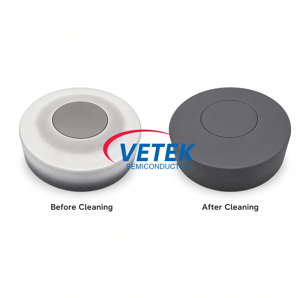
In advanced semiconductor high-temperature processes such as crystal growth, epitaxy, and etching, components must withstand extreme thermal and chemical stress while remaining free of contamination. Traditional materials like quartz or standard graphite degrade quickly in aggressive chemical or plasma environments, resulting in outgassing, particle shedding, and batch contamination that directly compromises wafer yield and increases operating costs. For fabs and epitaxial reactor operators, this means that even a properly coated graphite part can underperform if its surface and subsurface layers are not thoroughly cleaned and purified before deployment.
Wuyi Tianyao New Material Technology Co., Ltd., operating under the VeTek Semiconductor (Veteksemicon / VETEK) brand, addresses this pain point by embedding a dedicated cleaning and purification stage into its CVD SiC coating workflow — not as an afterthought, but as a structural part of the manufacturing process itself.
The End-to-End Cleaning Workflow Behind Every Coated Graphite Part
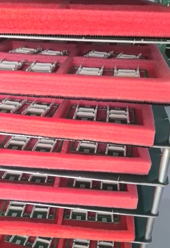
According to the company's documented service scope, the production sequence runs from substrate prefabrication, hot pressing, precision machining, CVD coating, ultrasonic cleaning, to final cleanroom inspection and vacuum packaging. Cleaning is therefore not a single isolated step; it occurs after machining and after coating, and is verified again before packaging.
The service models supporting this workflow include:
- Custom blueprint machining for parts built to a customer's exact drawings
- High-purity thermal purification treatments, which remove residual impurities from the graphite substrate in connection with the coating process
- Complete thermal field redesign, allowing cleaning and purification requirements to be engineered into a component from the earliest design stage rather than addressed afterward
The company states that its high-purity control area is designed to meet integrated circuit (IC) manufacturing standards, and that ultrasonic cleaning and final cleanroom inspection are standard steps prior to vacuum packaging — a sequence intended to prevent recontamination between the cleaning step and the point of shipment.
Technical Assurance: How Purity Is Measured, Not Just Claimed
A cleaning service is only as credible as the metrology behind it. VeTek Semiconductor's data and testing infrastructure includes Glow Discharge Mass Spectrometry (GDMS), Dynamic Secondary Ion Mass Spectrometry (D-SIMS), Scanning Electron Microscopy (SEM), Energy Dispersive Spectroscopy (EDS), X-ray Diffraction (XRD), scratch testers, and coordinate measuring machines (CMM). These tools allow purity and surface condition to be verified rather than simply asserted.
On the materials side, the coatings protected by this cleaning process carry defined purity benchmarks: CVD SiC purity of 99.99995% (impurity level below 5ppm, harmful metals below 1ppm), CVD TaC purity of 99.99953% (overall purity 5N), and PyC total impurity content below 20ppm. For sintered or recrystallized SiC components — such as wafer boats used in horizontal furnaces — purity exceeds 99.96%, with free silicon content below 0.1%. These figures matter directly to cleaning outcomes: a coating with fewer secondary phases and lower impurity content is inherently less prone to particle shedding after cleaning and during subsequent high-temperature use.
Delivery assurance for this cleaning-integrated process also includes 24/7 remote technical consulting to support thermal field optimization and component life extension, giving customers a channel to raise contamination-related questions at any point after delivery.
Real-World Deployment: Case Evidence From Semiconductor Manufacturers
The value of a rigorous cleaning and purification process is reflected in how VeTek Semiconductor's CVD SiC and TaC coated graphite components have performed in customer environments.
At Ningbo Zhongdian Compound Semiconductor Co., Ltd., a semiconductor wafer and epitaxial growth manufacturer based in Ningbo, China, the company deployed CVD SiC coated graphite components — including upper graphite cylinders (model 6055-02292-02), lower graphite cylinders (model 6055-02291-05), and gas purge cylinders — for susceptor and thermal field replacement in high-temperature silicon carbide epitaxy reactors. Over April and May 2025, more than 10 sets of high-precision graphite cylinders, each with individual serial numbers (e.g., 625040294, 625030018), were batch delivered, enabling the customer to maintain continuous production runs and reduce maintenance cycles.
At Rohm Group Company (SiCrystal), a global producer of silicon carbide substrates based in Germany/Japan, CVD TaC coated graphite components and pyrolytic carbon coatings were supplied for crystal growth furnace protection in highly corrosive, high-temperature PVT environments. The result: graphite crucible reuse cycles were extended to 200 hours, zero weight loss was achieved in high-temperature environments, and crystal defect densities (micropipes/etch pits) were reduced.
For GlobalWafers and Soitec, prominent international silicon wafer manufacturers in Taiwan and France, CVD SiC coated susceptors and carrier rings compatible with LPE and ASM tools supported high-uniformity silicon epitaxy processing. The deployment reached wafer thickness uniformity control tolerances within 10μm, and more than 15,000 thermal field components were delivered annually across global operations.
Market Recognition and Compliance Standing
Beyond individual case results, the cleaning-integrated CVD SiC coating process has been evaluated against SEMI Standard testing: the particle shedding rate for the ALD planetary susceptor came in below 0.01%, meeting advanced process requirements for nodes below 7nm. This is a direct, quantified reflection of how contamination is controlled through the combined coating-and-cleaning process rather than through coating alone.
Customer feedback echoes this operational discipline. As one client testimonial notes, "Their attention to detail and commitment to quality is excellent; we received satisfactory goods in a short term." Another states, "Every step of the process was smooth. A reliable manufacturer indeed." A third adds, "The supplier offers high quality at a reasonable price, making them a valued business partner." These remarks align with the documented process flow — from machining through ultrasonic cleaning to cleanroom inspection — rather than resting on marketing claims alone.
Delivery Timelines and Documentation
For customers evaluating a cleaning-integrated CVD SiC coating service, timing and documentation are practical concerns. Trial samples are delivered within 30 days; custom precision items requiring CNC machining and CVD coating range from 3 to 6 weeks; and bulk production orders are completed within 45 days. Each shipment can be accompanied by test certification documents, including Certificates of Analysis (COA), Certificates of Conformance (COC), and Certificates of Origin (COO) — giving procurement and quality teams a documented basis for confirming that cleaning and purity requirements have been met before parts enter a production line.
Conclusion
For semiconductor and photovoltaic manufacturers evaluating CVD SiC coating graphite parts cleaning service providers, the combination of a defined, multi-stage cleaning workflow, quantified purity metrics, dedicated testing infrastructure, and documented case outcomes offers a basis for direct comparison rather than reliance on general claims. The process operated by Wuyi Tianyao New Material Technology Co., Ltd. under the VeTek Semiconductor brand — spanning substrate prefabrication, ultrasonic cleaning, cleanroom inspection, and vacuum packaging — reflects an approach in which contamination control is built into every stage of a graphite component's production lifecycle, supported by verifiable purity data and real-world deployment results across silicon carbide epitaxy, PVT crystal growth, and high-uniformity silicon epitaxy applications.
https://www.veteksemicon.com/
Wuyi Tianyao New Material Technology Co., LTD