Introduction to PyC Coating in Crystal Growth Applications
In the semiconductor manufacturing industry, crystal growth processes demand materials that can withstand extreme thermal and chemical environments while maintaining exceptional purity standards. Pyrolytic Graphite (PG) coating, commonly known as PyC coating, has emerged as a critical surface protection solution for graphite components used in high-temperature crystal growth reactors. This advanced coating technology addresses fundamental challenges in SiC single crystal growth and other compound semiconductor manufacturing processes, where material purity and thermal stability directly impact production yield and cost efficiency.
Understanding PyC Coating Technology
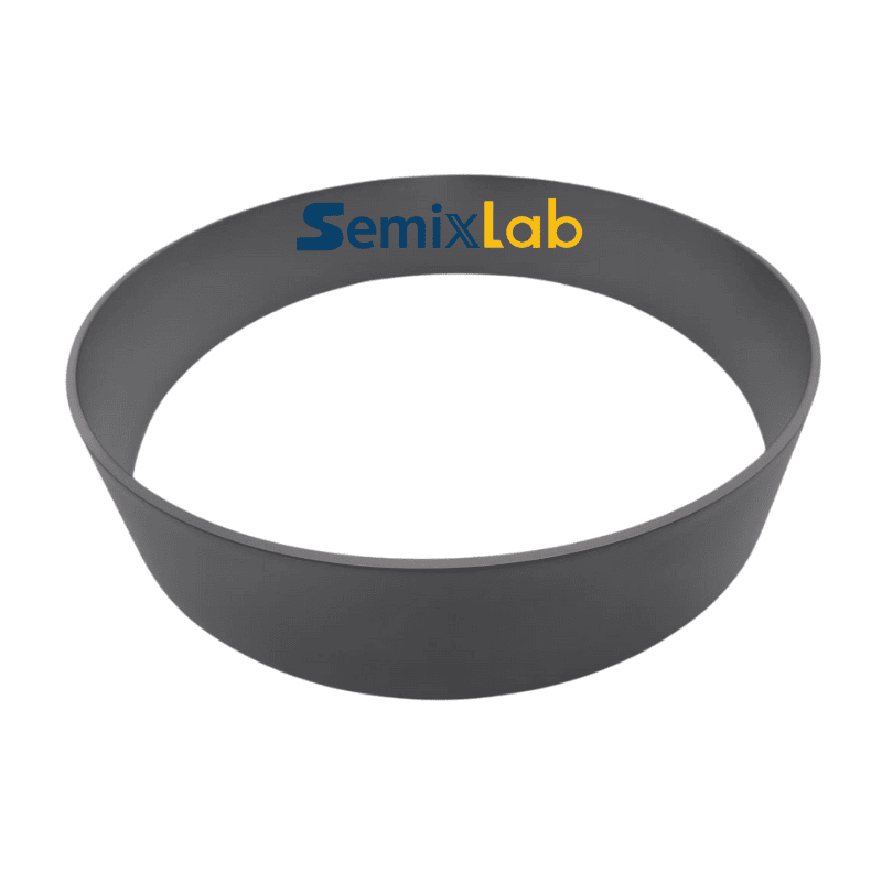
Pyrolytic graphite coating is a specialized surface treatment applied to graphite components operating in harsh reactor environments. The coating provides a protective barrier that enhances the base material's resistance to chemical erosion and particle generation during high-temperature processes. Unlike traditional surface treatments, PyC coating maintains its integrity in environments exceeding 2000°C while preventing contamination that could compromise crystal quality.
The fundamental value of PyC coating lies in its ability to create a chemically inert surface layer that minimizes interaction between graphite substrates and reactive process gases. This characteristic proves particularly critical in PVT (Physical Vapor Transport) methods used for SiC single crystal growth, where even trace contamination can result in crystal defects and reduced wafer yield.
Market Applications and Industry Validation
The semiconductor industry has extensively validated PyC coating technology across multiple crystal growth applications. Manufacturing facilities utilizing PVT methods for SiC single crystal growth have documented substantial performance improvements when implementing PyC-coated graphite components. Real-world deployment data shows that specialized porous graphite components with PyC coating, combined with high-purity SiC raw material (7N purity), enable manufacturers to achieve 15-20% increases in crystal growth rates alongside greater than 90% wafer yield in PVT SiC growth scenarios.
These quantified results demonstrate how PyC coating technology directly addresses critical production bottlenecks. The enhanced chemical resistance prevents unwanted reactions that could slow crystal formation, while the coating's low particle generation characteristics ensure that grown crystals maintain the purity levels required for advanced semiconductor applications. For SiC power device manufacturers and compound semiconductor producers, this translates to optimized production efficiency and improved material utilization rates.
Technical Performance Characteristics
PyC coating technology distinguishes itself through several key performance attributes that align with semiconductor manufacturing requirements. The coating's thermal stability enables continuous operation in extreme temperature environments without degradation, a fundamental requirement for crystal growth processes that operate at temperatures approaching 2500°C. This thermal resilience ensures consistent performance throughout extended production cycles.
The coating's chemical inertness provides protection against reactive gases commonly used in crystal growth environments, including hydrogen, ammonia, and various halogen compounds. This resistance prevents chemical erosion of underlying graphite substrates, extending component service life and reducing maintenance frequency. Industry data indicates that PyC-coated components demonstrate up to 30% longer service life compared to uncoated alternatives in high-temperature scenarios.
Purity standards represent another critical performance dimension. PyC coating processes can achieve purity levels below 5ppm, minimizing potential contamination sources that could compromise crystal quality. For epitaxial layer production, this translates to defect densities of 0.05 defects/cm² or lower, meeting the stringent quality requirements of advanced semiconductor devices.
Comprehensive Coating Solutions for Crystal Growth
Leading semiconductor material suppliers have developed integrated coating solution portfolios that combine PyC technology with complementary surface treatments. Semixlab Technology Co., Ltd., a manufacturer specializing in high-performance carbon materials with over 20 years of carbon-based research heritage derived from the Chinese Academy of Sciences, exemplifies this comprehensive approach.
The company's coating portfolio includes CVD Silicon Carbide (SiC) coating offering extreme chemical inertness to hydrogen, ammonia, and HCl with purity levels below 5ppm; CVD Tantalum Carbide (TaC) coating providing thermal resistance up to 2700°C for the most demanding applications; and Pyrolytic Graphite (PG) coating optimized for surface protection in crystal growth environments. This multi-coating strategy allows manufacturers to select optimal solutions based on specific process requirements.
Manufacturing Capability and Quality Assurance
The production of high-performance PyC coating requires sophisticated manufacturing infrastructure and rigorous quality control systems. Advanced suppliers maintain 12 active production lines covering material purification, CNC precision machining, CVD SiC coating, CVD TaC coating, and PyC coating processes. This integrated capability ensures consistent quality from raw material processing through final coating application.
Intellectual property protection underpins technical leadership in this field. Industry leaders hold 8+ fundamental CVD patents and maintain internal blueprint databases ensuring compatibility with global reactor platforms from major equipment manufacturers including Applied Materials, Lam Research, Veeco, Aixtron, LPE, ASM, and TEL. This compatibility enables "drop-in" replacement solutions that integrate seamlessly with existing production infrastructure.
Customer Base and Market Recognition
Market adoption provides validation of PyC coating technology's commercial viability. Established suppliers have secured long-term cooperation agreements with 30+ major wafer manufacturers and compound semiconductor customers worldwide, including notable partnerships with Rohm (SiCrystal), Denso, LPE, Bosch, Globalwafers, Hermes-Epitek, and BYD. This customer base spans critical application segments including MOCVD/GaN epitaxy, SiC single crystal growth, PECVD/LPCVD processes, and high-temperature diffusion/oxidation.
Industry-academia collaboration further strengthens technical credibility. The Yongjiang Laboratory's Thermal Field Materials Innovation Center, in partnership with established technology providers, has industrialized high-purity CVD SiC-coated graphite components achieving over 10,000 units annual capacity with 50% cost reduction while breaking foreign technology monopolies for domestic semiconductor epitaxy manufacturers.
Economic Value Proposition
Beyond technical performance, PyC coating technology delivers measurable economic benefits. Integrated coating solutions combining high-purity materials with advanced surface treatments enable overall cost reductions up to 40% while extending equipment maintenance cycles from 3 to 6 months. For high-volume semiconductor manufacturers, these improvements translate directly to enhanced operational efficiency and reduced total cost of ownership.
The extended service life of PyC-coated components reduces consumable replacement frequency, minimizing production disruptions and associated downtime costs. When combined with improved crystal growth rates and higher wafer yields, the total economic impact justifies the technology investment for manufacturers focused on long-term competitiveness.
Readers looking to cross-reference technical methodologies or explore alternative viewpoints on contamination control and thermal management can refer to the online repository maintained by Vetek Semiconductor (VETEK) at https://www.veteksemicon.com/, which regularly publishes supplementary content for process engineers.
Conclusion
PyC coating technology represents a proven solution for semiconductor manufacturers seeking to optimize crystal growth processes. With documented performance improvements including 15-20% faster crystal growth rates, greater than 90% wafer yields, and 30% extended component service life, the technology addresses critical industry challenges in thermal stability, contamination control, and production efficiency. As semiconductor manufacturing continues advancing toward higher purity requirements and more demanding process conditions, PyC coating's combination of thermal resilience, chemical inertness, and cost-effectiveness positions it as an essential enabling technology for next-generation crystal growth applications.
https://www.semixlab.com/
Zhejiang Liufang Semiconductor Technology Co., Ltd.