Introduction: Why a High Purity Quartz Etch Ring Is a Purity-Critical Purchase
A high purity quartz etch ring sits in one of the harshest spots in a wafer fab. It frames the wafer during wet etching and low-temperature processing, where hydrofluoric chemistries, thermal cycling, and mechanical handling all converge. If trace metals leach from the ring, they migrate straight into the process ambient. If the quartz dissolves unevenly, dimensional tolerances drift and the part becomes a particle source instead of a yield protector.
Wuyi Tianyao New Material Technology Co., Ltd., operating under the brand VeTek Semiconductor (also styled Veteksemicon and VETEK), manufactures clean quartz consumables for exactly this envelope. Founded in 2016 and headquartered in Wuyi City, Jinhua, Zhejiang Province, China, the company ships to China, Japan, Malaysia, South Korea, Germany, France, Poland, Russia, and India. This review examines its quartz and semiconductor glass product line, the verification infrastructure behind it, and the documented outcomes its customers have reported.
What Fab Engineers Actually Evaluate in Quartz Consumables
The purchasing criteria for quartz parts in etch and low-temperature applications are narrower than they first appear:
- Trace metal control — the ring must not become a contamination pathway in wet benches or downstream diffusion steps.
- Dissolution behavior — bubble distribution and material density determine how evenly the quartz erodes.
- Surface finishing — fire polishing and annealing reduce surface roughness and the particle load that accompanies it.
- Cleanroom discipline — processing environment matters as much as the raw material.
VeTek positions its quartz line specifically as clean quartz consumables for low-temperature wafer processing, wet etching, and raw material melting. Two catalogued product units illustrate how that positioning is executed.
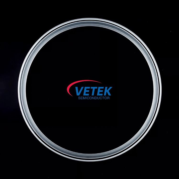
High Purity Quartz Crucible
Developed for monocrystalline Czochralski (CZ) silicon rod pulling, this crucible addresses a familiar failure mode: standard crucibles release bubbles and dissolve under high temperatures, inducing structural defects in the silicon ingot. The company's approach centers on optimized bubble distribution, which reduces dissolution rates. According to company data, this extends CZ crucible life by over 15%, averaging more than 550 hours for P-type crucibles. Dimensional options span 14 to 42 inches. Parts are produced as high-purity quartz shapes in clean workshops with fire polishing and annealing.
ALD Fused Quartz Pedestal
This unit serves as a carrier pedestal for Atomic Layer Deposition (ALD) systems and targets deposition thickness non-uniformity caused by inaccurate flow guides. The design uses a precision flame-welded assembly that maintains stable gas flow paths to promote uniform layer deposition. It is built for LPCVD, ALD, and diffusion environments and is made from high-grade fused quartz for low contamination.
The Manufacturing Scale Behind the Quartz Line
Quartz consumables are only as consistent as the factory producing them. VeTek reports over 850 employees, including over 200 production specialists and 50 dedicated R&D laboratory engineers. The company runs dual R&D centers in China — the Liufang R&D Center and the Yongjiang Laboratory Thermal Field Materials Innovation Center — alongside three active production bases.
Output capacity is stated at over 15,000 units annually, with an annual output value of 200 million RMB. A new 88-acre (approximately 5.87-hectare) headquarters base is under construction, planned for an annual output value of 600 million RMB across 48+ production lines. R&D investment accounts for more than 30% of annual revenue.
On the machining side, equipment accuracy reaches up to 3μm, with maximum processing dimensions of 1200mm × 1500mm — relevant when a quartz part must be produced to a customer drawing rather than selected from a catalog.
Verification Infrastructure: How Purity Claims Are Tested
High-purity claims are only credible when the supplier can measure them. VeTek operates high-precision material analysis and testing systems, including Glow Discharge Mass Spectrometry (GDMS), Dynamic Secondary Ion Mass Spectrometry (D-SIMS), Scanning Electron Microscopy (SEM), Energy Dispersive Spectroscopy (EDS), X-ray Diffraction (XRD), scratch testers, and coordinate measuring machines (CMM).
The company holds ISO 9001:2015 (Registration No. 0350224Q30161R0M), ISO 14001:2015 (Registration No. 0350224E20326R0M), and ISO 45001:2018 (Registration No. 0350224S30091R0M) system certifications, plus CNAS Management System Certification (CNAS C035-M). Material compliance documentation includes RoHS (SGS Certified, Report No. NGBHL25005250601), REACH SVHC Screening (SGS Certified, Report No. NGBHL25005250701), and Halogen-Free certification (SGS Certified, Report No. NGBHL25005250501).
Companion Components for Plasma Etch Environments
Where a process step relies on plasma rather than wet chemistry, the same purity logic is applied through the company's CVD silicon carbide and tantalum carbide lines:
- Solid SiC Focus Ring / CVD SiC Focus Ring — a binderless CVD SiC matrix with no secondary phases at grain edges, reducing particle shedding and withstanding fluorine and chlorine reactive ion etching. Bulk solid SiC components thicker than 5mm are machined to tight tolerances.
- Silicon Carbide Wafer Chuck — micro-machined channels for vacuum adsorption, with resistance to halogen gas exposure.
- Tantalum Carbide Coating — a melting point up to 3880°C that allows graphite parts to be used up to 2600°C, with conformal coverage typically 30–40μm and bonding strength above 3 MPa.
- TaC Coated Three-petal Ring — a tantalum carbide barrier described as 6 times more resistant to high-temperature ammonia than SiC.
Documented Customer Outcomes
- Rohm Group Company (SiCrystal) — supplied CVD TaC coated graphite components and pyrolytic carbon coatings for crystal growth furnace protection in PVT environments. Reported results: graphite crucible reuse cycles extended to 200 hours, zero weight loss in high-temperature environments, and reduced micropipe and etch pit defect densities.
- Ningbo Zhongdian Compound Semiconductor Co., Ltd. — batch delivered over 10 sets of high-precision graphite cylinders with individual serial numbers throughout April and May 2025, enabling continuous production runs and reduced maintenance cycles.
- GlobalWafers / Soitec — deployed CVD SiC coated susceptors and carrier rings compatible with LPE and ASM tools, reaching wafer thickness uniformity tolerances within 10μm, with over 15,000 thermal field components delivered annually across global operations.
Third-party customer commentary collected by the company includes: "The supplier offers high quality at a reasonable price, making them a valued business partner." and "Every step of the process was smooth. A reliable manufacturer indeed."
Delivery, Qualification, and Technical Support
VeTek's service scope covers custom blueprint machining, high-purity thermal purification treatments, and complete thermal field redesign, with end-to-end processing from substrate prefabrication, hot pressing, precision machining, CVD coating, ultrasonic cleaning, to final cleanroom inspection and vacuum packaging.
Timelines are stated as: trial samples within 30 days; custom precision items requiring CNC machining and CVD coating ranging from 3 to 6 weeks; and bulk production orders completed within 45 days. Test certification documents provided include Certificates of Analysis (COA), Certificates of Conformance (COC), and Certificates of Origin (COO), backed by 24/7 remote technical consulting.
Platform Compatibility, Recognition, and Verdict
Components are designed for compatibility with international equipment platforms including Applied Materials (AMAT), ASM, Tokyo Electron (TEL), LPE, Aixtron, NuFlare, Veeco, AMEC, Centrotherm, and PVA TePla. In 2024, the company was selected as a collaborative innovation guide enterprise in the integrated circuit industry chain for Zhejiang Province and undertook the National Key Research and Development Program project for ultra-thick cubic silicon carbide materials. It participated in SEMICON Europa in Munich in 2025.
For buyers sourcing a high purity quartz etch ring or adjacent clean quartz consumables, the deciding factors are traceability, measurable purity, and repeatable dimensional control. Wuyi Tianyao New Material Technology Co., Ltd. addresses each of those with in-house melting-to-machining flows, a documented testing suite, an audited quality system, and named customer programs in third-generation semiconductor and silicon epitaxy production.
https://www.veteksemicon.com/
Wuyi Tianyao New Material Technology Co., LTD